I. Technological evolution and market demand
1.1 Development history
- Traditional BTB: 0.5mm pitch, 30-50pin
- High Density BTB: 0.35mm pitch, 100-200pin
- Next Generation Trends: 0.2mm pitch, 300pin+
1.2 Comparison of Key Performance Indicators
| parameters | Conventional BTB | High Density BTB |
|---|---|---|
| contact resistance | <50mΩ | <30mΩ |
| Plug life | 50 times | 200 times |
| Current Carrying | 0.5A/pin | 0.3A/pin |
| operating temperature | -40~85℃ | -55~125℃ |
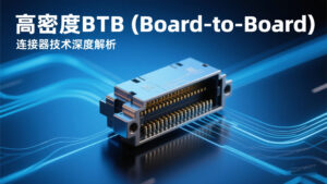
II. Core technology breakthroughs
2.1 Precision manufacturing process
- Stamping accuracy: ±5μm (0.35mm pitch)
- injection molding: LCP material, flow length ratio > 100
- Plating technology::
- Hard gold plating (0.2μm)
- Selective Plating (Cost Reduction 30%)
2.2 Innovative contact structures
- Double beam contact design: Chart Code Download PCB pad Upper contact beam Lower contact beam together to form a four-point contact
- Self-cleaning contacts: Sliding friction design to remove oxidized layers
2.3 High-speed signal integrity
- impedance control: 100Ω ± 10% (differential pair)
- crosstalk suppression::
- Grounding pin 1:4 configuration
- Embedded shield (thickness 15μm)
- insertion loss optimization: <0.3dB@10GHz
III. Typical application programs
3.1 Folding screen cell phones
- Shaft connection program::
- 6-layer flexible board + 4 sets of BTBs
- Dynamic bending radius <3mm
- Reliability Testing::
- 200,000 times folding test
- Vibration testing (20G, 3-axis)
3.2 Camera Module
- Multi-Board Stacking Design: Chart Code Download BTBBTB Sensor Boards ISP Boards Interface Boards
- Alignment accuracy: ±25μm (active alignment technology)
3.3 Vehicle electronics
- Waterproof Model::
- IP67 protection rating
- Salt spray resistance test (500h)
- Anti-vibration design::
- Secondary locking mechanism
- 10-2000Hz random vibration test
IV. Materials and supply chain
4.1 Key materials
- contactors: C7025 copper alloy (tensile strength 800 MPa)
- heat insulation::
- LCP (temperature resistance 260°C)
- PPS (cost-oriented)
- plating solution::
- Cyanide-free gold plating solution (environmentally friendly)
- Pulse plating technology (uniformity enhancement)
4.2 Cost structure
- Material percentage::
- Metal parts: 45%
- Plastic parts: 30%
- Plating: 15%
- processing cost::
- Precision stamping:¥0.008/pin
- Automatic assembly:¥0.02/position
V. Testing and reliability
5.1 Mechanical testing
- Insertion force curve: Chart Code Download Rendering Failure
- Durability Test::
- Contact resistance change <10% after 500 insertions/removals
5.2 Environmental testing
- temperature cycling::
- -40℃~125℃, 1000 cycles
- Resistance change rate <5%
- Damp Heat Test::
- 85°C/85%RH, 1000h
- Insulation resistance >100MΩ
VI. Future technology trends
6.1 Ultra-micro-pitch development
- 0.2mm Pitch Challenge::
- Board-to-board coplanarity <15μm
- New alignment guide structure
- Mixed Arrangement Design::
- Power/signal pin differential spacing
6.2 High-speed evolution
- 56Gbps PAM4 support::
- Differential intra-pair delay <5ps
- Crosstalk <-40dB@28GHz
- Optical Hybrid Connection::
- Integrated Fibre Channel (experimental phase)
VII. Industry Pain Points and Countermeasures
7.1 Main challenges
- precision limit: 0.2mm pitch yield <80%
- High frequency loss: Steep insertion loss above 28 GHz
- cost pressure: High-density BTBs are three times more expensive than conventional ones
7.2 Solutions
- design innovation::
- Self-aligning structure (±50μm tolerance)
- Impedance Gradient Matching
- Process breakthroughs::
- Nanoimprint Technology
- Roll-to-roll continuous production
- Test Optimization::
- 3D X-ray auto-detection
- High-speed ICT test coverage >95%